Methods of characterization of materials / sixth part
Greetings again science loving friends and welcome to my new installment of materials characterization, where I share my knowledge and experiences in the area of materials physics, especially semiconductor compounds.
The characterization of semiconductor materials is a fundamental tool for the creation of diverse optoelectronic devices. During my stay at Steem I have dedicated myself to sharing my experiences in this beautiful area of materials science. These experiences are based on the study of the physical and chemical properties of semiconductor compounds.
Next I am going to show you a technique very used by us to know the electrical properties of a semiconductor material, especially the electrical resistivity, mobility and concentration of charge carriers.

But first I recommend you to read my previous installments in order to understand a little better what I'm talking about.
Here I will leave you the links:
Part 1 Part 2 Part 3 Part 4 Part 5Recently I have focused on writing about some of the techniques most used to determine electrical resistivity in a semiconductor material, in reality there are many and all of them have basically the same purpose, which is to find the mobility, concentration of charge carriers of a material, where we involve different terms such as electrical conductivity, the hall coefficient, energy gap, etc., etc. ... All these techniques going through different paths (when we talk about mathematical development of equations), but they fulfill the same purpose which is to determine the "most important electrical properties of a semiconductor material".
Van der Pauw's technique is another used to find the electrical resistivity, mobility and concentration of charge carriers in a semiconductor material. It is named after its creator, and unlike the techniques previously explained, "Van der Pauw" uses the surface resistance of the sample to determine the values of mobility and concentration in the material, remembering that in the former we use the hall coefficient and conductivity at room temperature. This implies several advantages for the technique that we are going to develop next, since one of the main ones is that we can obtain mobility measurements of load carriers at different temperatures, whereas in the previous one we can only do it at room temperature. There is also no dependence on the cross section of the sample or the length of the same to perform their calculations, which has the great advantage of using different geometries of the sample and this minimizes errors when it comes to measurement. It also allows the confirmation of the ohmic contacts of the sample on its surface which also reduces errors and we can obtain reliable results.
But maybe we will ask ourselves: if with the previous techniques we can also obtain all these important values in the electrical characterization of a material, why are we going to use this new technique? Isn't it the same?
The answer to this question is very simple:
Basically different methods or techniques of characterization are used depending on the need of the scientist, that is to say, several factors can influence as the environment, equipment, viability, but the most important one is without a doubt the geometry of the sample.
When we synthesize a semiconductor compound independently of the growth method, at the end we obtain a stone as it is observed in the (figure 1). This stone must later be cut or sliced into different portions in order to be used in different characterization methods (electrical, optical, structural, morphological), and these require a different preparation of the sample. This is why in order to make the most of the ingot, it must be cut into several portions, but sometimes some of these portions are unusable due to their irregular shape and it is here where the Van der Pauw technique plays an important role and it is to use this portion of the sample with irregularities and to be able to prepare it for electrical measurements. Next I am going to explain how this technique is and what is needed to make measurements of electrical resistivity in a semiconductor.
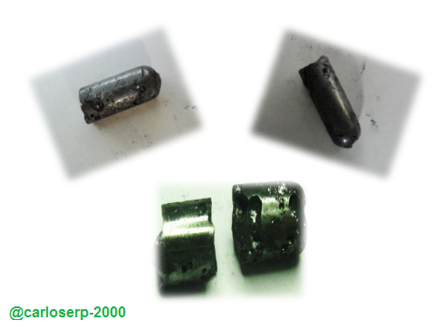
Figure 1: Small stone or ingot of a semiconductor compound after synthesis
It is recommended to create thin samples in the form of plates in order to adjust them to the required geometry. The mean diameters (D) of the contacts, and the thickness of the sample (d) should be much smaller than the distance between the contacts (L). Relative errors caused by D values other than zero are of the order of D/L (figure 2).
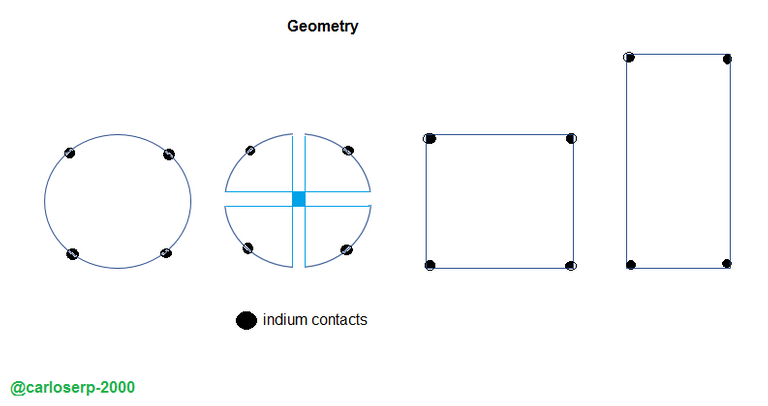
Figure 2. Sample geometries required for resistivity and Hall effect measurements using Van der Pauw's technique
However, for a sample of uniform thickness, the resistivity of the layer without taking into account the geometric parameters of the sample; with the same contact arrangement, you can also perform a Hall effect measurement to derive the mobility of the load carriers. That is, the measurement of surface resistivity is based on a conformal transformation of the domain consisting of the sample into a semi-plane, whose origin is the image of the edge of the sample. To obtain accurate results it is necessary to have very small contacts with respect to the size of the sample and placed on its edges as can be seen in the (figure 3).
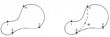
Figure 3. Example of an arbitrary sample for electrical resistivity and Hall effect measurements using the Van de Pauw technique
As I mentioned the sample can be arbitrary, it is recommended that you have some of the geometries in Figure 2, actually it is preferable to be circular, and I say this from my own experience because the results of the measurements are more effective in this geometric form.
The contacts must be in a suitable position, i.e. they must be of the same length with respect to each other, otherwise measurement errors may occur.
In addition we must take into account some important factors that must have the semiconductor sample, such as: The sample must be correctly synthesized, by this I mean to be free of holes in its interior, as well as the surface must be clean and completely polished without presenting any corrosive agent, the contacts must be perfectly welded in the corners of the sample so that these at the time of receiving high temperature can not be detached from the sample, the thickness must be approximately constant and small with respect to its extension.
It is very important to remember that to use this method is that the four contacts are ohmic, ie the current that circulates through the contacts is proportional to the voltage applied in them.
In addition to the materials necessary for sample preparation, which are fine and coarse copper wire, indium and tin dots, as well as bakelite that serves as a sample holder, which I will not show in this publication, since it is the same procedure used in the measurements with the techniques shown above, perhaps later you can show a more sophisticated method for placing the samples.
The following instruments are required for Hall effect measurements using the Van der Pauw technique:
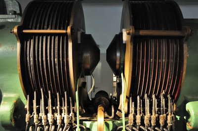
Public domain Flickr

Public domain Pixabay
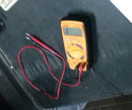
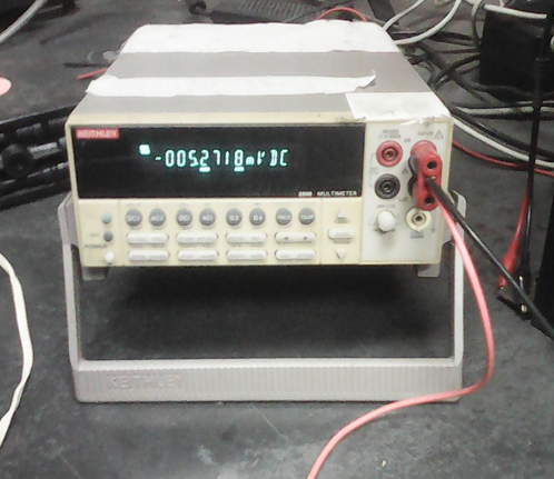
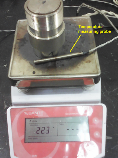
The experimental configuration for the measurement system must then be carried out as shown in the following diagram.
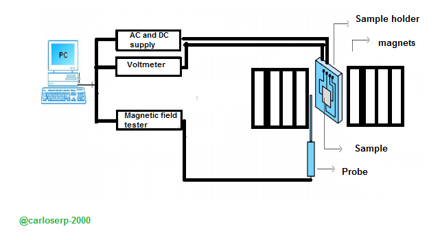
Diagram of the electrical resistivity and Hall effect measurement system using Van der Pauw's technique
And this publication is just a word of what I'm going to share in my next installment. Where I will show a system of measurements elaborated by me where I demonstrate the hall effect using different techniques of sample preparation, as well as how is the process of calculation by means of the Van der Pauw technique.
Sources
Publish through our official app and you will get an extra vote of 5% https://www.steemstem.io/

 Video credits @gtg
This post has been rewarded with an upvote from city trail as part of Neoxian City Curation program
 . We are glad to see you using #neoxian tag in your posts. If you still not in our discord, you can join our Discord Server for more goodies and giveaways.
Do you know that you can earn NEOXAG tokens as passive income by delegating to @neoxiancityvb. Here are some handy links for delegations: 100SP, 250SP, 500SP, 1000SP. Read more about the bot in this post. Note: The liquid neoxag reward of this comment will be burned and stake will be used for curation.
Thank you @neoxian-city for support
Congratulations @carloserp-2000! You have completed the following achievement on the Steem blockchain and have been rewarded with new badge(s) :
You can view your badges on your Steem Board and compare to others on the Steem Ranking
If you no longer want to receive notifications, reply to this comment with the word
STOPVote for @Steemitboard as a witness to get one more award and increased upvotes!
This post has been voted on by the SteemSTEM curation team and voting trail. It is elligible for support from @curie and @minnowbooster.
If you appreciate the work we are doing, then consider supporting our witness @stem.witness. Additional witness support to the curie witness would be appreciated as well.
For additional information please join us on the SteemSTEM discord and to get to know the rest of the community!
Thanks for having used the steemstem.io app and included @steemstem in the list of beneficiaries of this post. This granted you a stronger support from SteemSTEM.
Thank you dear bot ;)